{var%20f='http://v.t.sina.com.cn/share/share.php?appkey=1515056452',u=z||d.location,p=['&url=',e(u),'&title=',e(t||d.title),'&source=',e(r),'&sourceUrl=',e(l),'&content=',c||'gb2312','&pic=',e(p||'')].join('');function%20a(){if(!window.open([f,p].join(''),'mb',['toolbar=0,status=0,resizable=1,width=440,height=430,left=',(s.width-440)/2,',top=',(s.height-430)/2].join('')))u.href=[f,p].join('');};if(/Firefox/.test(navigator.userAgent))setTimeout(a,0);else%20a();})(screen,document,encodeURIComponent,'','','https://www.xiaopingtou.cn//data/attach/topic/topicKPo7gB.jpg', '推荐 qq374432723 的文章《Intel 中断控制器8259A》','https://www.xiaopingtou.cn/article-62555.html','页面编码gb2312|utf-8默认gb2312'));)
- Programmable Interrupt Controller (PIC) 8259A
The Intel 8259A Programmable Interrupt Controller handles up to eight vectored priority interrupts for the CPU.It is cascadable for up to 64 vectored priority interrupts without additional circuitry. The PIC functions as an overall manager in an Interrupt-Driven system environment. It accepts requests from the peripheral equipment, determines which of the incoming requests is of the highest importance (priority), ascertains whether the incoming request has a higher priority value than the level currently being serviced, and issues an interrupt to the CPU based on this determination. Each peripheral device or structure usually has a special program or ‘‘routine’’ that is associated with its specific functional or operational requirements; this is referred to as a ‘‘service routine’’. The PIC, after issuing an Interrupt to the CPU, must somehow input information into the CPU that can ‘‘point’’ the Program Counter to the service routine associated with the requesting device. This ‘‘pointer’’ is an address in a vectoring table and will often be referred
to, in this document, as vectoring data. Block Diagram:

重要模块分析:
-
INTERRUPT MASK REGISTER (IMR)
The IMR stores the bits which mask the interrupt lines to be masked. The IMR operates on the IRR. Masking of a higher priority input will not affect the interrupt request lines of lower quality. -
IRR/ISR register
The interrupts at the IR input lines are handled by two registers in cascade, the Interrupt Request Register (IRR) and the In-Service (ISR).- The IRR is used to store all the interrupt levels which are requesting service;
- The ISR is used to store all the interrupt levels which are being serviced.
-
CASCADE BUFFER/COMPARATOR
This function block stores and compares the IDs of all 8259A’s used in the system. The associated three I/O pins (CAS0-2) are outputs when the 8259A
is used as a master and are inputs when the 8259A is used as a slave. As a master, the 8259A sends the ID of the interrupting slave device onto the CAS0–2 lines. The slave thus selected will send its preprogrammed subroutine address onto the Data Bus during the next one or two consecutive INTA pulses.

2.INTERRUPT SEQUENCE
The powerful features of the 8259A in a microcomputer system are its programmability and the interrupt routine addressing capability. The latter allows
direct or indirect jumping to the specific interrupt routine requested without any polling of the interrupting devices. The normal sequence of events during an
interrupt depends on the type of CPU being used.The events occur as follows in an MCS-80/85 system:
- One or more of the INTERRUPT REQUEST lines (IR7–0) are raised high, setting the corresponding IRR bit(s).
- The 8259A evaluates these requests, and sends an INT to the CPU, if appropriate.
- The CPU acknowledges the INT and responds with an INTA pulse.
- Upon receiving an INTA from the CPU group, the highest priority ISR bit is set, and the corresponding IRR bit is reset. The 8259A will also release a CALL instruction code (11001101) onto the 8-bit Data Bus through its D7–0 pins.
- This CALL instruction will initiate two more INTA pulses to be sent to the 8259A from the CPU group.
- These two INTA pulses allow the 8259A to release its preprogrammed subroutine address onto the Data Bus. The lower 8-bit address is released at the first INTA pulse and the higher 8-bit address is released at the second INTA pulse.
- This completes the 3-byte CALL instruction released by the 8259A. In the AEOI mode the ISR bit is reset at the end of the third INTA pulse. Otherwise, the ISR bit remains set until an appropriate EOI command is issued at the end of the interrupt sequence.
This sequence is timed by three INTA pulses.
- During the first INTA pulse the CALL opcode is enabled onto the data bus.

- During the second INTA pulse the lower address of the appropriate service routine is enabled onto the data bus. When Interval e 4 bits A5–A7 are programmed, while A0–A4 are automatically inserted by the 8259A. When Interval e 8 only A6 and A7 are programmed, while A0–A5 are automatically inserted.

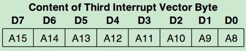
- During the third INTA pulse the higher address of the appropriate service routine, which was programmed as byte 2 of the initialization sequence (A8–A15), is enabled onto the bus.
3.Interrupt priorities
The BIOS typically initializes the 8259A chip to use a scheme with fxed priorities: the device on IRQ0 has the highest priority and the device on IRQ7 has the lowest priority.
They are both cleared after the contents of the flag register are stacked during an interrupt. When the IF bit is set, it allows the INTR pin to cause an interrupt; when the IF bit is cleared, it prevents the INTR pin from causing an interrupt. When IF = 1, it causes a trap interrupt (interrupt type number 1) to occur after each instruction executes. This is why we often call trapping a single step. When TF = 0, normal program execution occurs. The interrupt flag is set and cleared by the STI and CLI instructions, respectively. There are no special instructions that set or clear the trap flag. 参考资料:
https://blog.csdn.net/longintchar/article/details/79439466